
How is a PCB Board Used in Consumer Electronics?
3 min readPCB Board Used in Consumer Electronics
Consumer electronics PCBs are a key component of the gadgets that make up a world in which many people live, work and play. They enable the smartphones, tablets and computers that we rely on to function correctly, and are responsible for creating the options and possibilities that come with modern devices.
Without the development of printed circuit boards, these technologies would have been prohibitively expensive and inaccessible. Post-war PCBs allowed computers to be miniaturized and affordable, bringing high-tech capacity and capability to everyday consumers. They also made it possible for home stereos, televisions and video games to become popular and mainstream.
Before the invention of the pcb board, all electronic components were connected by wires. This was inefficient, because the connections could easily get tangled and created reliability problems. It was also difficult to debug a device when it failed. PCBs, which are flexible and modular, solved these issues.
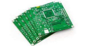
How is a PCB Board Used in Consumer Electronics?
The first step in the process of making a PCB is to create a schematic diagram. This diagram shows the pin pads of all the components on the board and their connections to each other. It is then converted to a CAD file that can be used to produce the final product.
Once the CAD file is completed, the components are mounted on the PCB. This can be done in two ways: through-hole or surface mount. Through-hole mounting involves the use of wire leads that are passed through holes in the PCB and soldered to copper traces on the opposite side of the board. Surface mount technology, on the other hand, uses components with metal leads that are attached to copper traces on the same side of the board as they are.
After the components are mounted, the PCB is sent for inspection. During this process, an operator inspects the copper traces using a camera that can see through the layers of substrate material (typically FR-4 glass epoxy). This is important because the traces need to be free from defects and corrosion. The inspected board is then ready to proceed to the next stage of production.
Rigid PCBs can be single-sided, double-sided or multilayered. They can be thin or thick, and are usually constructed from a dielectric composite of an epoxy resin with a woven, non-woven or cotton paper reinforcement. The most common insulating substrate material is fiberglass, although other materials are also used.
In addition to checking the copper traces for defects, an operator will look at the overall appearance of the board. This will help them determine if it is the correct shape and size for its intended application. The board may also undergo an optical inspection to verify its quality. This involves taking pictures of the copper traces and comparing them to the PCB design files.
During this stage, the operator will also cover areas that should not be soldered with solder mask. This is typically a green color but can be one of several other colors. The solder mask is imaged on the PCB with a dry film, exposed to light and developed. The unexposed areas are then washed away, leaving the solder mask covering the area that should be plated or etched.
